The following program computes the square (k*k) of a positive integer k, stored in location 0x4000 and stores the result in location 0x4002.
(The result is to be treated as a 16 bit unsigned number).
Assumptions:
- A memory access takes 5 cycles
- The system call initiated by the HALT instruction takes 20 cycles to execute. This does not include the number of cycles it takes to execute the HALT instruction itself.
        .ORIG X3000
        AND R0, R0, #0
        LEA R3, NUM
        LDW R3, R3, #0
        LDW R1, R3, #0
        ADD R2, R1, #0
LOOP    ADD R0, R0, R1
        ADD R2, R2, #-1
        BRP LOOP
        STW R0, R3, #1
        HALT
NUM     .FILL x4000
        .END
- How many cycles does each instruction take to execute on the LC-3b microarchitecture described in Appendix C?
- How many cycles does the entire program take to execute? (answer in terms of k)
- What is the maximum value of k for which this program still works correctly?
- How will you modify this program to support negative values of k? Explain in less than 30 words.
- What is the new range of k?
	State 18: MAR <- PC, PC <- PC + 2
        State 33: MDR <- M
        State 35: IR <- MDR
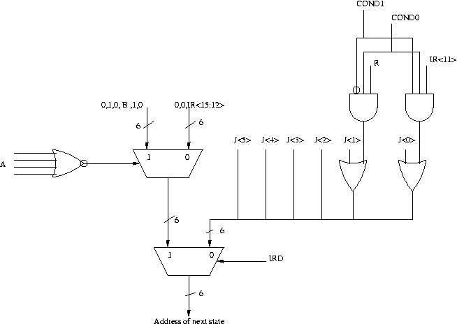
Which of the following different organizations would still work
correctly, why or why not? (Assume that a memory access takes five
cycles).
	State 18: PC <- PC + 2
	State 33: MAR <- PC, MDR <-M
	State 35: IR <- MDR
	State 18: MAR <- PC
	State 33: PC <- PC + 2, MDR <-M
	State 35: IR <- MDR
	State 18: MAR <- PC
	State 33: MDR <- M
	State 35: IR <- MDR, PC <- PC + 2
2.Suppose we want to get rid of the BEN register altogether. Can this be done? If so, explain how. If not, why not? Is it a good idea? Explain.
3.Suppose we took this further and got rid of state 0. The figure below shows a modified microsequencer. What is the 4-bit signal denoted as A in the figure? What is the 1-bit signal denoted as B?
Assembler format for PUSH:
PUSH SR
Encoding:
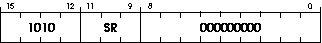
Operation:
R6 = R6 - 2;
MEM[R6] = SR;
Description:
SR is pushed onto the stack.
Example:
PUSH R1
Assembler format for POP:
POP DR
Encoding:
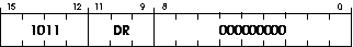
Operation:
DR = MEM[R6];
setcc(DR);
R6 = R6 + 2;
Description:
Top word is popped off the stack and loaded into DR. Condition codes
are set based on the value loaded into DR.
Example:
POP R1
Your job:
A. Append the current state machine for supporting PUSH and POP
instructions.
B. Will the current datapath support the above state machine? If
not, then draw the new datapath to implement the above state
machine. Show the new structures you added to support PUSH and POP
operations.
C. Are there any additional control signals needed for the new
states? If so, what are they? Give the values of these new control
signals in each new state you added and show them clearly in your
datapath figure for Part B.
D. How many cycles will each of the following set of instructions
take to execute?
1. PUSH R4
2. ADD R6, R6, # -2
STW R4,
R6, #0
3. POP R0
4. LDW R0, R6, #0
ADD R6, R6,
#2
- 16-bit address in MAR. This signal can take the following values: xFE00, xFE02, xFE04, xFE06, and OTHER (any other address between x0000 and xFDFF).
- 1-bit control signal R.W. The access is a read access if this signal is R, write access if it is W.
- 1-bit control signal MIO.EN. If this signal is 1, a memory or I/O access should be performed in this cycle.
The logic has five outputs:
- 1-bit MEM.EN signal. Memory is enabled if this signal is 1.
- 2-bit select signal for INMUX. This signal can take the following values: KBDR, KBSR, DSR, MEMORY.
- 1-bit LD.KBSR signal. KBSR will be load-enabled at the end of the current cycle if this signal is 1.
- 1-bit LD.DDR signal. DDR will be load-enabled at the end of the current cycle if this signal is 1.
- 1-bit LD.DSR signal. DSR will be load-enabled at the end of the current cycle if this signal is 1.
Your task is to draw the truth table for this Address Control Logic. Mark don't care values with X in your truth table. Use the conventions described above to denote the values of inputs and outputs. Please read Section C.6 in Appendix C on Memory-mapped I/O before answering this question. Also, refer to Appendix A to find out the addresses of device registers.
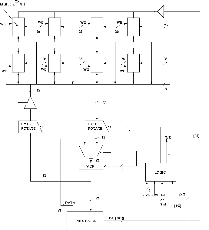
Construct the truth table to implement the
LOGIC block, having inputs SIZE, R/W, 1st or 2nd access,
PHYS_ADDR[1:0] and the outputs shown in the above figure. Assume that
the value of SIZE can be Byte (00), HalfWord (01), and Word
(10). Clearly explain what function each output serves.
-------------------------------------------------
Show the logic required to implement the block labeled LOGIC that is specified by section C.5.1.